DMAPS R&D

While covering key roles for the design and construction of the CMS pixel detector upgrades, the group of Prof. Wallny also develops novel detector concepts for future experiments. Experiments at any future accelerator will have to cope with all or a subset of the following challenges: high spatial granularity, precise timing, very low material budget, and low power consumption. We concentrate the R&D in two fields:
- diamond as leakage current free and radiation hard sensor material, and
- Depleted Monolithic Active Pixel Sensors (DMAPS).
Hybrid pixel detectors used for the CMS experiment provide excellent performance due to two silicon entities, the read out chip and the sensor that are independently optimized for performance, and interconnected in a post-processing step. The interconnection of the two entities is laborious and requires minimal thicknesses of the sensor and readout-chips for mechanical stability.
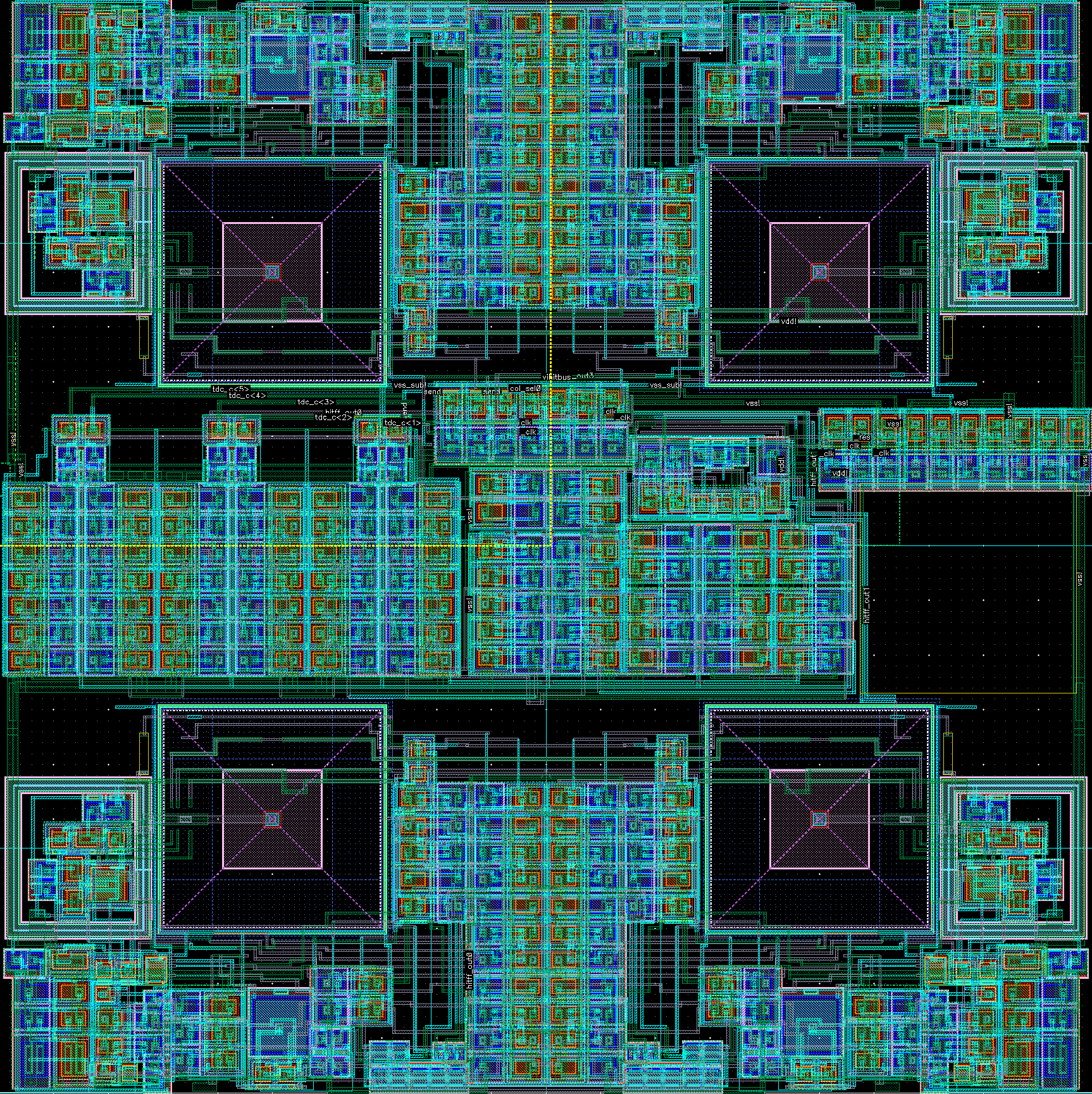
In our DMAPS project we work on the implementation of the readout electronics and sensing diode in the same portion of silicon. First prototypes exist and show promising performance. The current work targets the optimization of the design: precise time resolution with high granularity and radiation hardness. These optimizations require in-depth understanding of the physics of the signal generation in combination with the invention of — among others — elegant electronics solutions for signal amplification, low-power and precise time-to-digital conversion.
